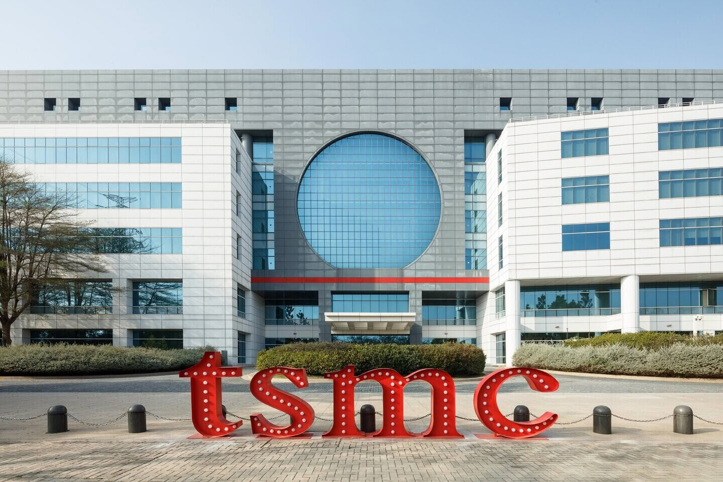
Taiwan Semiconductor Manufacturing Company (TSMC) is rapidly accelerating the capacity expansion for its groundbreaking 1.4-nanometer node. According to whispers within the supply chain, the semiconductor behemoth plans to construct four state-of-the-art 1.4-nanometer wafer fabrication facilities situated in the Central Taiwan Science Park. TSMC aims to achieve formidable large-scale production capabilities by the second quarter of 2028. However, since official executives have yet to unveil a definitive production timetable for these new foundries, this timeline remains industry speculation.
New Fabrication Plants Target AI and High-Performance Computing
The highly anticipated 1.4-nanometer manufacturing process, officially designated as A14, represents TSMC’s next monumental leap following its 2-nanometer node. Publicly available intelligence suggests that the Central Taiwan Science Park initiative encompasses four distinct manufacturing facilities. A select few of these plants might initiate preliminary trial production as early as 2027, subsequently scaling up their output capacity.
Nevertheless, industry research analysts propose that the initial facilities, temporarily codenamed P1 and P2, could enter the production phase ahead of schedule. Conversely, the completion of the P3 facility is projected for the second quarter of 2028, while the P4 plant might not commence operations until the fourth quarter of that year. Therefore, asserting that all four foundries will simultaneously launch in early 2028 appears slightly inaccurate, as the crucial transition from trial runs to mass production naturally demands considerable time. For further details on these developments, one can consult the recent industry analysis detailing TSMC expansion plans.
TSMC previously affirmed that the A14 development is progressing flawlessly, with prominent clients already expressing profound interest for applications spanning smartphones, artificial intelligence, and high-performance computing. Within its comprehensive annual report, the corporation noted that constructing these 1.4-nanometer foundries empowers them to agilely address the surging demand for advanced nodes, largely driven by the explosive growth of AI technologies.
Strategic Pricing for the Advanced A14 Node
Interestingly, supply chain rumors indicate that a single A14 wafer might cost approximately 35,000 dollars, which is only marginally higher than the current 33,000-dollar price tag for a 2-nanometer wafer. If these whispers prove accurate, it signifies that TSMC has deliberately avoided establishing a vast pricing chasm between the A14 and 2-nanometer foundry services. This calculated strategy likely aims to leverage highly competitive pricing to entice developers of AI chips, server processors, and premium mobile silicon.
Alternatively, this modest price increment might suggest that the performance leap from the 2-nanometer node to the A14 architecture is not extraordinarily massive. Cultivating advanced manufacturing processes, from initial research to full-scale production, demands colossal financial investments. Had the A14 fabrication process involved vastly superior complexity and delivered unprecedented performance gains, TSMC would undoubtedly have established a significantly higher price point.
Support Our Threat Intelligence
If you find our technology report and cybersecurity news helpful, consider supporting our work.
 Buy Me a Coffee
PayPal
Buy Me a Coffee
PayPal