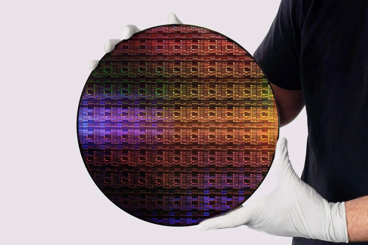
IBM officially announced the successful fabrication of the world’s inaugural sub-1-nanometer semiconductor chip. This groundbreaking process node reaches an astonishing 7 angstroms, equivalent to 0.7nm. The chip employs a revolutionary architecture dubbed “Nanostack.” Consequently, IBM has unprecedentedly packed nearly 100 billion transistors onto a silicon wafer the size of a fingernail. This achievement firmly illuminates the trajectory for high-performance computing and energy-efficient semiconductor development over the next decade.
From Nanosheet to Nanostack: The Zenith of 3D Stacking
Reflecting upon 2021, IBM previously unveiled a 2nm process technology utilizing a “Nanosheet” architecture. The newly introduced Nanostack paradigm represents a profound evolutionary leap built directly upon that foundational technology.
To overcome the physical limitations of inadequate planar space, IBM’s research and development team engineered a solution. They discovered they could vertically stack and interlace these nanosheet transistors. According to the technical architectural diagrams released by IBM, the design features several incredible specifications:
- Atomic-Scale Miniaturization: Each individual transistor comprises three distinct nanosheet components. Each sheet measures a mere 5nm in thickness, with a minuscule 9nm gap separating them.
- Extreme Thinness: Under intense microscopic scrutiny, each nanosheet layer fundamentally consists of exactly 15 rows of silicon atoms.
Through this sophisticated 3D volumetric stacking technique, IBM successfully doubled the transistor density. The 0.7nm process chip accommodates twice the density of their previous 2nm process design.
A Dual Leap in Performance and Energy Efficiency
The exponential doubling of transistor density directly precipitates a remarkable enhancement in computational efficiency. IBM highlighted that, compared to their predecessor 2nm process node, this novel 0.7nm chip offers developers two extreme configuration options:
- Performance Orientation: Achieves a staggering 50% increase in computational performance while maintaining identical energy consumption levels.
- Energy Efficiency Orientation: Secures a massive 70% reduction in energy consumption while delivering identical performance output.
Jay Gambetta, the Director of IBM Research, articulated a compelling vision. He stated that the new Nanostack architecture will catalyze a future characterized by vastly enhanced computational capacity without the accompanying explosion in power consumption. This development undoubtedly provides a massive boost for modern, power-hungry AI data centers and the training of immense large language models.
Navigating the Challenging Timeline to Mass Production
Despite this astonishing technological breakthrough, a long and arduous journey remains before achieving genuine commercial mass production.
Official IBM assessments estimate that the Nanostack architectural chips require approximately five additional years to reach large-scale manufacturing. However, the broader semiconductor industry generally perceives this timeline as overly optimistic.
Consider the case of Rapidus, a Japanese chip manufacturer and current IBM partner. Earlier this year, Rapidus announced its ambitious goal to initiate mass production of 2nm process chips by the latter half of 2027. Consequently, leaping directly into 0.7nm mass production within a few short years presents an immense challenge. The intricate coordination of manufacturing yields with cutting-edge lithography equipment, specifically High-NA EUV, will be a monumental test for the industry.
Support Our Threat Intelligence
If you find our technology report and cybersecurity news helpful, consider supporting our work.