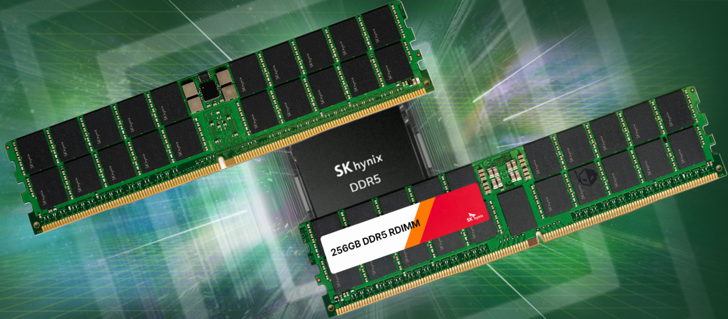
South Korean memory titan SK Hynix recently reiterated at a prominent industry symposium that the artificial intelligence sector fundamentally cannot exist without advanced memory solutions. As the artificial intelligence landscape continually evolves, the voracious demand for specialized memory hardware will undoubtedly remain robust. Consequently, SK Hynix plans to relentlessly fortify its technological supremacy by leveraging cutting-edge memory architectures, an expanding network of global production hubs, and state-of-the-art research and development facilities.
Strategic Roadmap: Advancing From HBM to HBF
High Bandwidth Memory (HBM) remains an indispensable companion for modern artificial intelligence accelerators. Since June 2026, SK Hynix has strategically supplied key clientele with elite 12-layer, 48GB HBM4E memory samples boasting a staggering single-pin velocity of up to 16Gbps. The manufacturer asserts that this formidable hardware enhances energy efficiency by an impressive 20 percent compared to the standard HBM4 architecture. Nevertheless, because these advanced HBM4E iterations remain strictly in the sampling phase, SK Hynix will continue collaborating intimately with its partners to drive mass production, though a definitive timeline remains unannounced.
Simultaneously, the enterprise is aggressively exploring High Bandwidth Flash (HBF) technology. Notably, SK Hynix previously partnered with SanDisk to unveil the inaugural HBF standard specifications. Utilizing NAND flash architecture, HBF positions itself uniquely between traditional high-bandwidth memory and solid-state drives. Its primary objective is to exponentially expand storage capacity while simultaneously delivering vastly superior bandwidth. However, because this high-bandwidth flash concept remains firmly embedded within the nascent research and development stages, the ultimate triumph of the technology and its subsequent market adoption remain subjects for future observation. For further insights into their strategic milestones, one can review how SK Hynix detailed its advanced memory roadmap.
Global Expansion Cycles Measured in Years
SK Hynix Chief Executive Officer Kwak Noh-Jung articulated that the corporation is actively constructing formidable production and research facilities across multiple global jurisdictions. During August, the enterprise commenced construction on the massive Y2 DRAM fabrication plant in Yongin and the sophisticated M17 NAND facility in Cheongju, representing a colossal capital injection of 54 trillion South Korean won.
Furthermore, SK Hynix is establishing a critical operational base in Indiana, United States. This facility will primarily execute the advanced packaging and rigorous testing procedures required for next-generation HBM modules. Current projections indicate that this facility will initiate mass production during the latter half of 2029; importantly, this specific plant will not fabricate raw DRAM wafers on American soil.
Support Our Threat Intelligence
If you find our technology report and cybersecurity news helpful, consider supporting our work.
 Buy Me a Coffee
PayPal
Buy Me a Coffee
PayPal