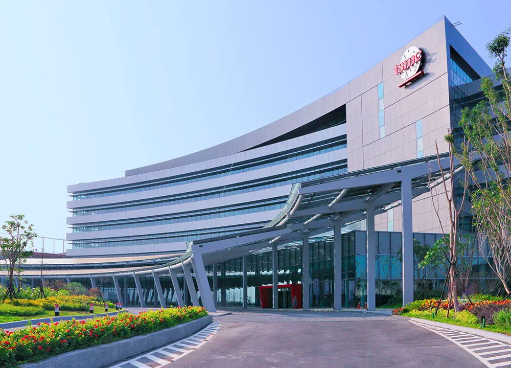
In February this year, TSMC confirmed the construction of its second wafer fab (Fab 2) in Japan. This expansion in capacity is expected to optimize the overall cost structure and supply chain efficiency. Additionally, TSMC held the inauguration ceremony for its first Japanese wafer fab (Fab 1) on February 24, 2024, with plans to commence mass production by the end of 2024.
According to Trendforce, Japan Advanced Semiconductor Manufacturing (JASM), a collaboration between TSMC, Sony, DENSO Corporation, and Toyota, has begun preparations for the construction of Fab 2 on the eastern side of Fab 1. The site covers approximately 321,000 square meters, 1.5 times the size of Fab 1. The project is estimated to cost around 2.2 trillion yen and, like its predecessor, has received support from the Japanese government, which will provide a subsidy of 732 billion yen.

Fab 2 is scheduled to break ground at the end of 2024 and begin operations by the end of 2027, focusing on 6/7nm process technology. In the future, the combined monthly production capacity of Fab 1 and Fab 2 is expected to exceed 100,000 12-inch wafers. The semiconductor manufacturing processes employed will include 40nm, 22/28nm, 12/16nm, and 6/7nm, catering to chips for the automotive, industrial, consumer, and high-performance computing (HPC) sectors. Capacity planning can be adjusted based on customer demand, and it is anticipated that over 3,400 high-tech jobs will be created directly.
Moreover, it has been reported that Kumamoto Prefecture’s new governor, Takashi Kimura, expressed in a recent media interview his commitment to persuading TSMC to establish a third wafer fab in the region. Additionally, he hopes to attract numerous semiconductor-related companies and research institutions to Kumamoto, transforming it into a semiconductor hub, including advancements in artificial intelligence (AI), data centers, and autonomous driving technology.


