At COMPUTEX 2024, AMD introduced the new Zen 5 architecture and unveiled consumer-grade processors based on this architecture, including the desktop Ryzen 9000 series and the mobile Ryzen AI 300 series processors. The Ryzen 9000 series exclusively utilizes Zen 5 cores, while the Ryzen AI 300 series employs a hybrid architecture, integrating both Zen 5 and Zen 5c cores.
Recently, AMD chip design engineer Mike Clark gave an interview to TomsHardware following the “AMD Tech Day 2024,” discussing the design of the Zen 5 architecture and addressing some concerns from enthusiasts.
It is well known that AMD’s approach to “big-little” cores differs from Intel’s. The Zen 5c core is essentially a low-power, streamlined version of Zen 5, using the same ISA but with a more compact design, achieving the same IPC and functionality with higher energy efficiency. The Zen 5c core occupies less space than the Zen 5 core but operates at lower frequencies, offering reduced peak performance compared to the standard Zen 5 core. This makes Zen 5c more suitable for mobile applications, where power consumption and thermal management are critical, which is why AMD has not yet adopted a hybrid architecture for desktop processors.
Mike Clark noted that hybrid architecture design presents challenges, such as achieving the correct frequencies, maintaining core count balance, and maximizing benefits within limited space. However, with improvements in Windows scheduling and increased experience, compact core designs like Zen 5c are expected to appear in desktop processors in the future, allowing for more cores within the same area and enhancing cost efficiency. AMD employs thread placement techniques to allocate lighter workloads to the compact cores.
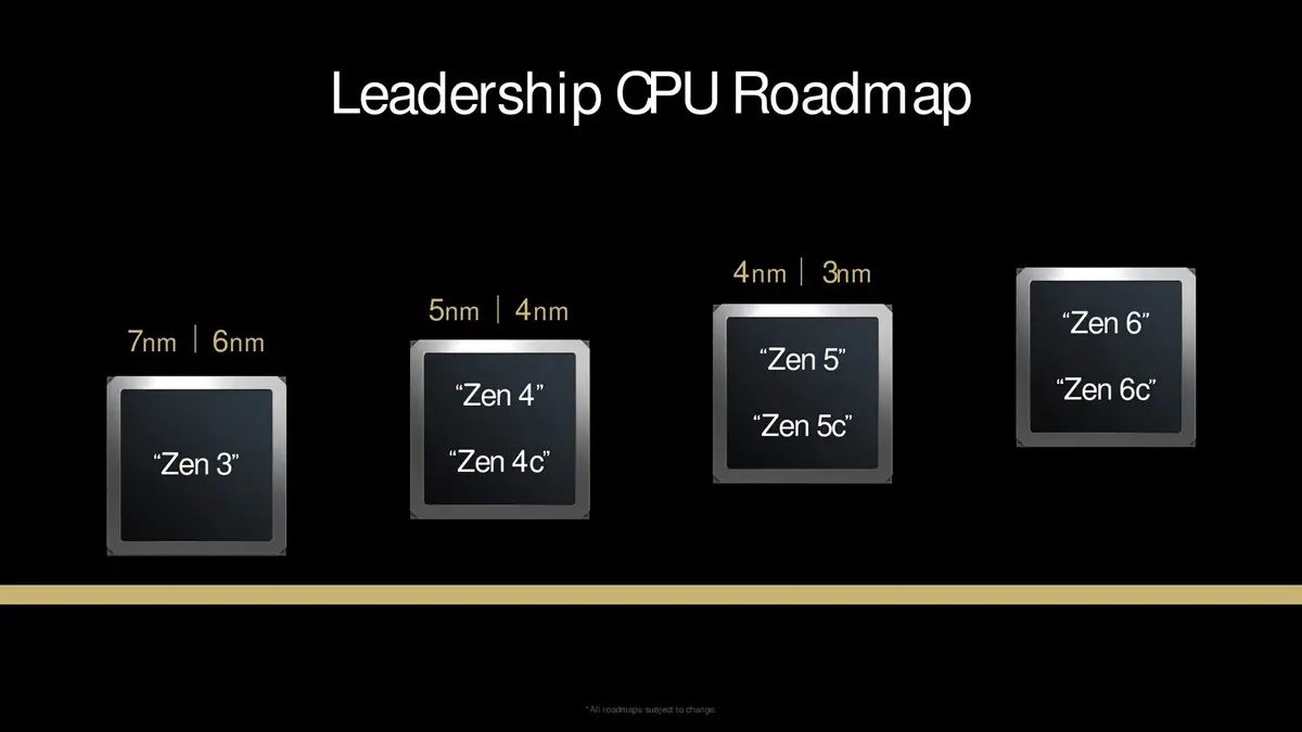
At “AMD Tech Day 2024,” AMD updated its technology roadmap, indicating that Zen 5 and Zen 5c are manufactured using 3/4nm processes. Based on current information, the initial CCDs based on Zen 5c and Zen 5 architectures use two different manufacturing processes, with the former being 3nm and the latter 4nm. This implies that AMD’s forthcoming major products, including Granite Ridge, Fire Range, and Turin’s Zen 5 architecture CCDs, are primarily built on the 4nm process.
Mike Clark explained that the showcased technology roadmap is flexible. When developing the Zen 5 architecture, AMD worked with both 3nm and 4nm process technologies. Regardless of the changes attempted, the inevitable reality is that 4nm consumes more power than 3nm and is challenging to manage alongside the distinct technologies and functionalities, impacting the planar layout. In practical application, this may be more difficult than anticipated. AMD will deliver 3nm and 4nm products in a short timeframe, essentially overlapping. The design teams worked separately on these products, requiring communication and collaboration to achieve consistency, which was highly challenging but ultimately successful. There remains significant room for improvement in the forthcoming Zen 6.
Zen 5 marks the first time the Ryzen series includes full AVX-512 acceleration, capable of running AVX-512 instructions at the same frequency as standard instructions—a feat Intel struggled with for a long time, often opting to run AVX-512 instructions at reduced frequencies or eventually abandoning them. Many are curious about how AMD achieved this.
Mike Clark believes the key to success was introducing AVX-512 when it was more balanced with the rest of the machine. While AVX-512 consumes more power, so does integer processing, with scheduling requiring substantial power consumption. AMD leveraged numerous sensors and used its firmware for dynamic management to respond more effectively. Clark is confident that Intel has also learned this lesson. Additionally, the Zen 5c core can also run full AVX-512 instructions.


