Recently, Western Digital introduced the BiCS8 2Tb QLC NAND flash memory at an investor event. This chip boasts the highest density in the industry, promising faster, larger, and more energy-efficient SSDs. Utilizing 218-layer BiCS8 FLASH 3D technology, it is remarkably compact, fitting easily on a fingertip.
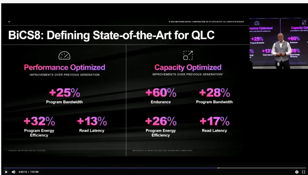
According to Tom’s Hardware, Western Digital shared extensive comparative performance data on the BiCS8 2Tb QLC NAND flash, highlighting improvements in power consumption, storage density, and I/O performance over competing flash products. Each flash die consists of multiple stacked NAND flash chips, meaning that storage manufacturers can offer 4TB in a single package by stacking 16 of these new flash chips. If mass production is achieved, it could redefine the cost of high-capacity SSDs.

Robert Soderbery, Executive Vice President and General Manager of Flash Business at Western Digital, expressed his excitement in unveiling this chip, designed to meet the storage needs of data centers and artificial intelligence (AI). Western Digital will soon announce this product, sharing with everyone the world’s largest capacity memory chip.
According to Western Digital, the BiCS8 2Tb QLC NAND flash has a density 15-19% higher than its competitors, an I/O interface speed 50% faster, and a program energy efficiency per GB of data 13% lower. Western Digital also detailed the manufacturing process, employing CBA (CMOS directly Bonded to Array) technology, where each CMOS wafer and cell array wafer are separately manufactured and then bonded together, akin to YMTC’s Xtacking architecture.


