Intel has confirmed that the latest Lunar Lake processors will have two modules manufactured by TSMC: the compute module using N3B technology and the platform control module using N6 technology. The true successor to the Core Ultra 100 is Arrow Lake, though Intel has disclosed little information about the fabrication process it will employ.

According to Digitimes, TSMC has already begun using the 3nm EUV FinFET process to produce chips for Intel’s new notebook processors, though it is unclear whether this pertains to Lunar Lake or Arrow Lake, as both target the laptop market. Arrow Lake features the same Lion Cove architecture P-Core and Skymont architecture E-Core as Lunar Lake, but their interconnects differ. Arrow Lake’s P-Core and E-Core are connected via a ring bus and share an L3 cache, unlike Lunar Lake.
The integrated graphics of Arrow Lake are said to be based on the Alchemist Xe-LPG+ architecture, a generation behind the Battlemage Xe2 architecture used in Lunar Lake. However, for this processor, aimed at mainstream and high-performance platforms, integrated graphics performance is less critical. The NPU is expected to meet the requirements of Microsoft’s Copilot+ AI PC, likely sharing similarities with Lunar Lake.
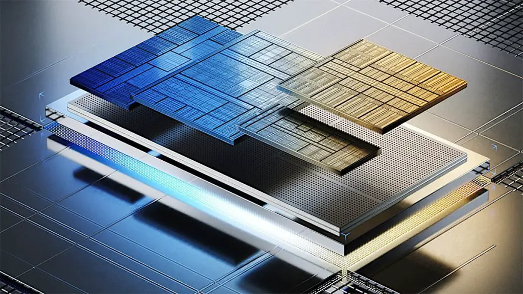
Reports as early as February suggested that Arrow Lake might use TSMC’s 3nm process for the graphics module. Given Lunar Lake’s reliance on TSMC for CPU cores, it is plausible that Arrow Lake’s compute module could also be outsourced to TSMC. A hybrid approach using both Intel 20A and TSMC N3 processes is also possible. With the introduction of Foveros advanced packaging technology, Intel’s consumer processors adopt a modular design, allowing for various combinations of different modules to create a diverse range of products.


