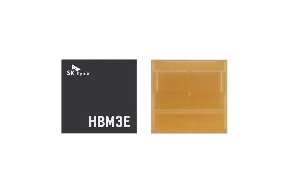
In recent years, artificial intelligence (AI), high-performance computing (HPC), and PCs have driven the development of high-performance DRAM products, with the market demand for HBM products rapidly increasing. Samsung, SK Hynix, and Micron, the three major memory manufacturers, have all intensified their investments. SK Hynix, currently the leader in the HBM sector, made its debut at COMPUTEX 2024, showcasing the latest HBM3E and MR-RUF technologies, stating that hybrid bonding will play a crucial role in chip stacking.

According to Trendforce, SK Hynix’s MR-RUF technology involves attaching semiconductor chips to the circuit, using EMC (liquid epoxy resin molding compound) to fill the gaps between the chips or between the chips and bumps. At this stage, MR-RUF technology enables tighter chip stacking, with a 10% improvement in thermal performance and energy efficiency, allowing for up to 12 layers of vertical stacking, offering products with a capacity of 36GB.
In contrast, Samsung and Micron employ TC NCF technology, which requires high temperatures and pressure to cure and remelt the materials, followed by cleaning. This process involves 2-3 steps, whereas MR-RUF technology can complete the entire process in one step without the need for cleaning. According to SK Hynix, the thermal conductivity of MR-RUF is approximately twice that of TC NCF, significantly impacting production speed and yield. Given the current market share, SK Hynix’s claims seem highly convincing.
Rumor has it that the JEDEC Solid State Technology Association may relax the height requirements for HBM4, specifically the maximum limit of 720 micrometers, allowing the height of 12-layer and 16-layer vertical stacked HBM4 to be increased to 775 micrometers. This would enable memory manufacturers to achieve 16-layer stacking with existing bonding technology, without transitioning to new hybrid bonding technology.
SK Hynix disclosed that in future chip stacking, bumps will be eliminated, and special materials will be used to fill and connect the chips. This material, similar to liquid or glue, will provide heat dissipation and chip protection, resulting in a thinner overall chip stack. SK Hynix is highly optimistic, believing that hybrid bonding technology could achieve stacking of over 20 layers within the 775-micrometer limit, without the need to transition to new processes.


