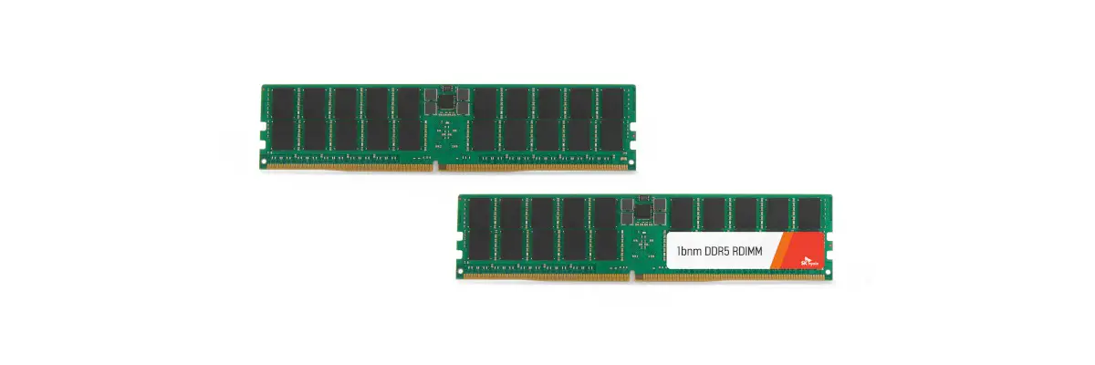
Previous reports indicated that SK Hynix is preparing to launch sixth-generation 10nm-class 1cnm process DRAM products, having already established customer certification and production plans, with mass production set for the third quarter of 2024. Compared to the existing fifth-generation 10nm-class 1β (beta) nm process, which also employs EUV lithography, the new process will produce more chips per wafer and achieve greater power efficiency.
According to The Elec, SK Hynix intends to use Inpria MOR photoresist for its 1cnm DRAM.

The 1cnm process DRAM from SK Hynix will feature five EUV layers, with one layer utilizing MOR technology for patterning. If SK Hynix proceeds with this decision, it will mark the first application of MOR photoresist in DRAM mass production. Samsung is considering a similar approach, planning to introduce Inpria MOR photoresist in their 1cnm DRAM, but SK Hynix is ahead of Samsung in the production timeline.
As early as 2022, SK Hynix collaborated with Samsung to research MOR technology. SK Hynix believes that metal oxide resists will enhance the performance of future DRAMs while reducing costs. Photoresists are used in the lithography process during chip production, where they chemically react to light, creating circuit patterns on the wafer.
It is understood that SK Hynix will expedite the compatibility verification process of its memory products with Intel’s data centers, ensuring that 1cnm DDR5 DRAM can swiftly enter the market and be promptly supplied to major customers like Amazon and Microsoft once mass production begins. Samsung plans to commence mass production of 1cnm DRAM products by the end of this year, aiming to obtain customer validation by December.


