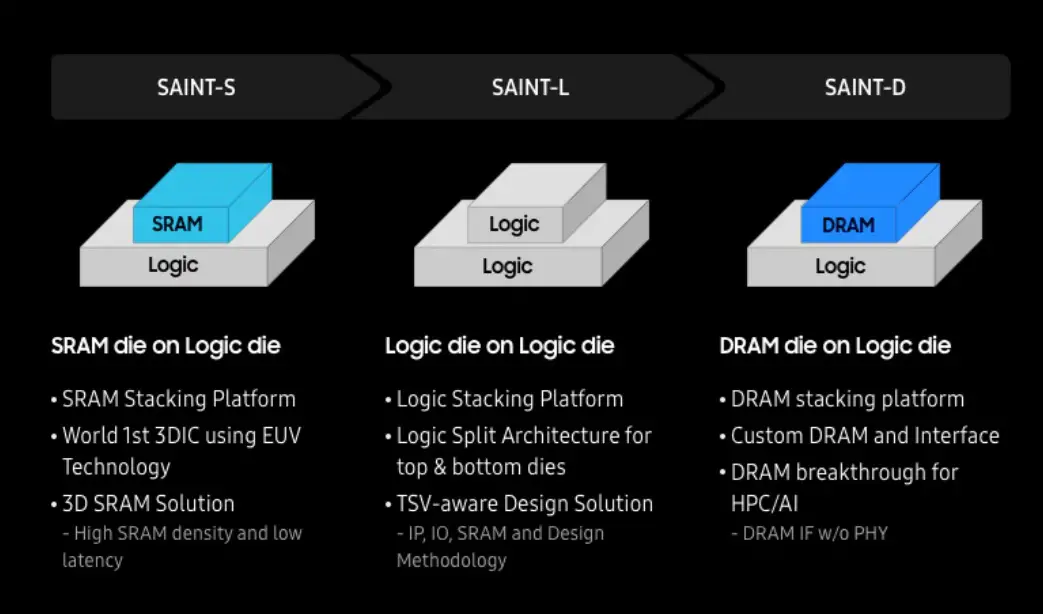
Last year, reports emerged that Samsung was preparing its 3D chip packaging technology, capable of integrating the logic and memory chips required for high-performance computing into a smaller footprint. Currently, HBM products primarily utilize 2.5D packaging technology, but Samsung plans to introduce 3D packaging technology with the debut of HBM4 in 2025.
According to TrendForce, Samsung confirmed at this month’s “Samsung Foundry Forum (SFF)” that it will launch 3D HBM packaging services within this year.

It is understood that Samsung’s advanced packaging solution, named “SAINT (Samsung Advanced Interconnection Technology),” aims to compete with TSMC’s CoWoS packaging. Samsung currently offers three packaging technologies:
- SAINT S – for vertically stacking SRAM memory chips and CPUs
- SAINT D – for the vertical packaging of CPUs, GPUs, DRAM, and other core IPs
- SAINT L – for stacking application processors (APs)
Under 2.5D packaging technology, HBM chips are horizontally connected to the GPU on a silicon interposer. By vertically stacking HBM chips on the GPU, 3D packaging technology can eliminate the need for a silicon interposer (a thin substrate located between chips that allows communication and cooperation between them).
It is understood that Samsung plans to offer 3D HBM packaging services in a “turnkey” manner. To achieve this, Samsung’s advanced packaging team will vertically interconnect HBM chips produced by its memory business unit with GPUs manufactured by its foundry division for chip design companies. Samsung hopes that through advanced packaging solutions, it can capture more market share from competitors, increase the shipment volume of its HBM products, and enhance its market competitiveness.


