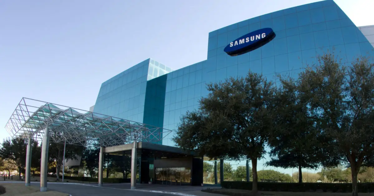
In May 2022, Samsung announced the construction of a new wafer fabrication plant in Taylor, Texas, with an initial investment of $17 billion. However, as the project progressed to the equipment procurement stage, the investment surged to $25 billion. This year, Samsung further increased the investment to $44 billion, nearly doubling the initial amount. The existing wafer plant in Austin, Texas, only advanced to the 14nm process; with the addition of EUV lithography equipment, it will advance to the 4nm process.

According to ETnews, Samsung has delayed equipment procurement orders for the new wafer plant in Taylor, deferring the final decision until the third quarter of 2024. As the demand for artificial intelligence (AI) hardware continues to rise, Samsung aims to upgrade the process from 4nm to 2nm to better compete with TSMC and Intel.
Samsung plans to establish a comprehensive advanced manufacturing ecosystem in Taylor, which will include two wafer fabrication plants, a research and development facility focused on technologies preceding current production nodes, and an advanced packaging facility for producing 3D high-bandwidth memory and 2.5D packaging. The first wafer plant is scheduled to commence operations in 2026, followed by the second in 2027, with the R&D facility also coming online that year. Over the next few years, Samsung is expected to invest more than $40 billion in Taylor, Texas, and the surrounding region, creating at least 21,500 jobs.
The U.S. Department of Commerce announced this year that it has signed a non-binding preliminary terms memorandum (PMT) with Samsung, providing approximately $6.4 billion in direct funding under the CHIPS Act. The scale of subsidies for Samsung under the CHIPS Act is second only to Intel ($8.5 billion) and TSMC ($6.6 billion). Unlike Intel and TSMC, however, Samsung has not received loans and guarantees from the CHIPS Act, while Intel and TSMC have secured $11 billion and $5.5 billion in loans, respectively.


