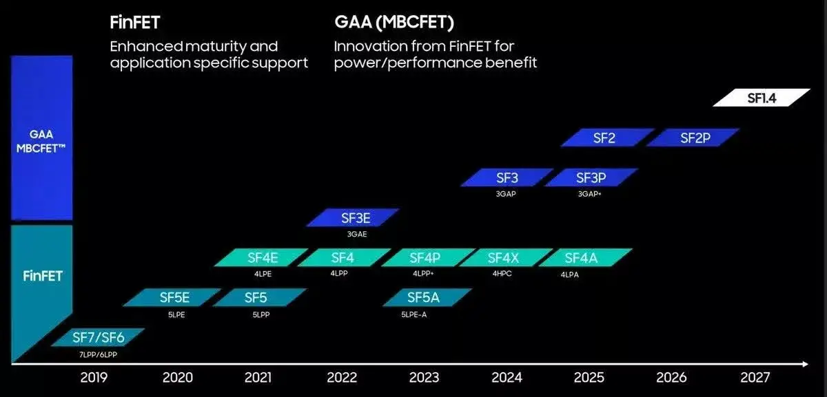
In 2022, at the “Samsung Foundry Forum 2022,” Samsung unveiled its future technological roadmap, including the plan to commence mass production of the 2nm (SF2) process in 2025. Last month, Samsung also announced a collaboration with Preferred Networks Inc. to provide comprehensive semiconductor solutions for the latter’s AI accelerator chips, utilizing the 2nm GAA process and 2.5D packaging technology known as Interposer-Cube S (I-Cube S).
According to The Elec, Samsung intends to increase the number of EUV exposure layers in its 2nm process by over 30% compared to its 3nm process, which currently uses 20 layers. Third-party reports indicate that TSMC employs 25 EUV layers in its N3 process. As the number of EUV layers rises, so does the manufacturing cost, potentially leading to a significant price increase for Samsung’s 2nm process.
Samsung first introduced EUV technology in its 7nm process in 2018 and has subsequently increased the number of EUV layers with each successive node. Currently, Samsung is also developing the 1.4nm (SF1.4) process, aiming for mass production in 2027, with an expected EUV layer count exceeding 30. Additionally, Samsung plans to increase the number of nanosheets in the 1.4nm process from three to four, further enhancing performance and power efficiency.
Beyond logic chips, Samsung has also employed EUV technology in memory chips, such as the sixth-generation 10nm-class 1cnm process, which uses six or seven EUV layers.


