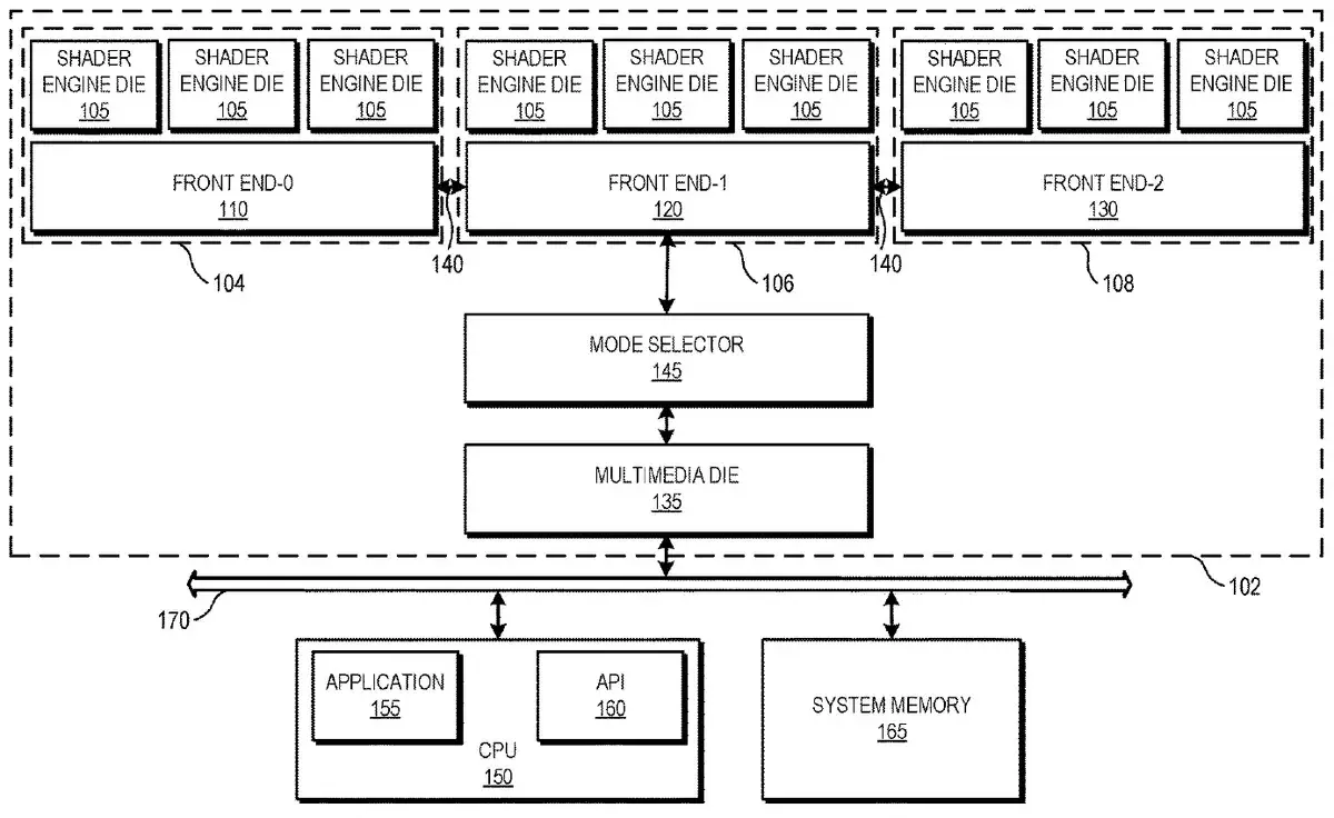
As chip design becomes increasingly complex and the cost of advanced processes rises, many chip companies are turning their attention to multi-chip designs to address the limitations of single-chip architectures. AMD is one such company. Currently, AMD employs multi-chip designs in its CPUs and GPUs and has long identified this as the future direction.
According to TomsHardware, a new patent submitted by AMD on December 8, 2022, and recently discovered, suggests that AMD is seeking to design small chips for a broader range of applications and to produce more complex multi-chip module GPUs.

In the current RDNA 3 architecture, AMD uses a Graphics Core Die (GCD) to achieve the primary functions of the GPU and multiple Memory Cache Dies (MCDs) to handle the memory interface and cache. In AMD’s new patent, the GPU is divided into several small chips that can be configured to operate either as a single GPU or as multiple GPUs working together. These GPU chips can run in three modes:
- The first mode, single GPU – All GPU chips work together as a unified GPU, sharing resources and collaboratively processing tasks. In this mode, typically, a single front-end chip manages the instruction scheduling for all shader engine chips within the GPU. This is essentially the traditional way GPUs operate.
- The second mode, multiple GPUs – The GPU chips are divided into different groups, each functioning as an independent GPU. Each group has its own front-end chip responsible for task scheduling for the associated shader engine chips.
- The third mode, hybrid configuration – This mode offers a flexible configuration where some GPU chips operate as a single GPU, while others function as independent GPUs.
From the description, this patent resembles the CDNA series architecture used in data center GPUs. However, based on past trends, it is likely to extend to consumer-grade products in the future.


