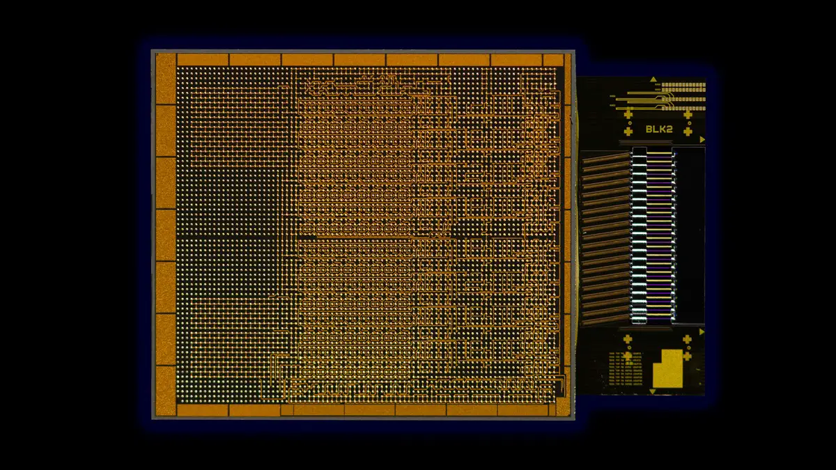
Intel Corporation’s Integrated Photonics Solutions (IPS) Group has demonstrated the industry’s first fully integrated optical compute interconnect (OCI) chiplet co-packaged with an Intel CPU and running live data. Intel’s OCI chiplet enables co-packaged optical input/output in emerging AI infrastructure for data centers and high performance computing applications. (Credit: Intel Corporation)
Researchers from the Massachusetts Institute of Technology (MIT) and collaborating institutions have developed a fully integrated photonic processor capable of performing key deep neural network computations optically, directly on-chip.
Modern deep learning models have grown so complex that they are approaching the limits of conventional electronic hardware. Photonic devices, which utilize light for computation, offer a faster and more energy-efficient alternative. However, previous iterations could not perform all types of neural network computations. Nonlinear operations required external electronic components, resulting in slower processing speeds and increased energy consumption.
This new device addresses these challenges. During testing, the photonic processor executed essential classification tasks in under half a nanosecond, achieving an accuracy exceeding 92%—on par with traditional electronic hardware.
The chip is composed of interconnected modules forming an optical neural network and was fabricated using commercial chip manufacturing processes. This breakthrough paves the way for scaling the technology and integrating it seamlessly with existing electronic systems.
The system operates by encoding the parameters of a deep neural network model into light. Programmable beam splitters perform matrix multiplications on input data, while nonlinear optical functional units (NOFUs) execute nonlinear functions. A portion of the light is redirected to photodiodes, which convert optical signals into electrical currents. This approach minimizes energy consumption and eliminates the need for external amplifiers.
The photonic system demonstrated over 96% accuracy during training and more than 92% accuracy in inference tasks, with all critical operations completed in under half a nanosecond.
Built on the standard infrastructure and manufacturing processes used for CMOS chip production, the device is primed for mass production with minimal error rates.
This photonic processor holds significant promise for computationally intensive tasks, including lidar systems, astronomical research, particle physics, and high-speed telecommunications. Additionally, it offers substantial potential for real-time data processing applications.
Future research will focus on scaling the device and integrating it with practical systems such as cameras and telecommunication equipment. The team will also explore algorithms designed to fully leverage the advantages of photonic data processing.
The project received partial funding from the National Science Foundation (NSF), the U.S. Air Force Office of Scientific Research, and NTT Research.


