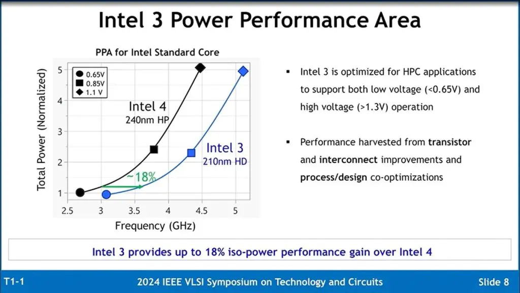
In the July 2021 “Intel Accelerated: Process and Packaging Technology Online Event,” Intel CEO Pat Gelsinger unveiled a roadmap of “five process nodes in four years,” driving Intel’s product development through 2025 and beyond. The third process node in this roadmap is Intel 3, which, through further FinFET optimization and increased use of EUV in more steps, achieves approximately an 18% performance-per-watt improvement and a 10% density enhancement over Intel 4.
According to TomsHardware, Intel has confirmed that the Intel 3 process has entered mass production at two facilities: one in Oregon, USA, and the other in Ireland. These factories are manufacturing the recently launched Xeon 6 series “Sierra Forest” and “Granite Rapids” processors, primarily aimed at data center products.
Intel has also provided new details about the Intel 3 process, the final generation of semiconductor technology employing FinFET transistors. This process delivers stronger performance and higher transistor density and supports ultra-high-performance applications with a 1.2V voltage. It is designed not only for Intel’s products but also for foundry customers, with continuous development planned for the coming years.
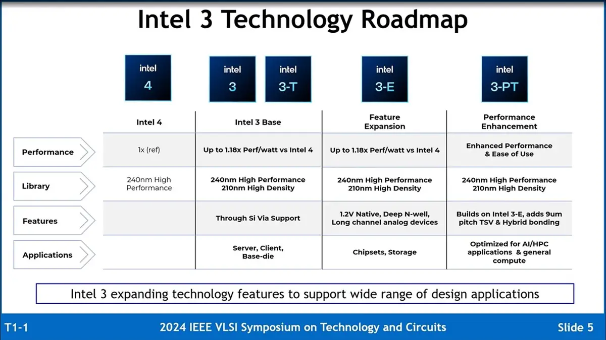
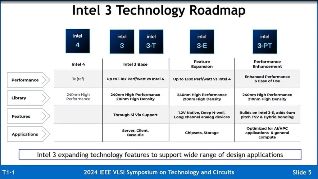
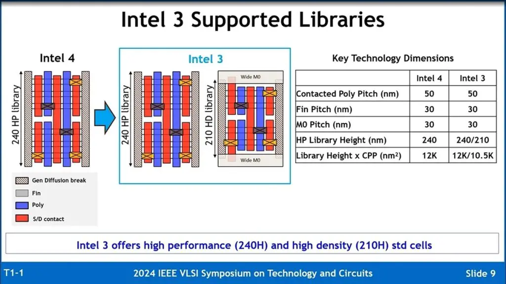
In addition to the standard version, Intel offers three variants: Intel 3T, Intel 3E, and Intel 3PT. The Intel 3T variant, supported by TSV, can serve as a foundational chip; Intel 3E provides enhanced functionality for chipset and storage applications; Intel 3PT offers further performance enhancements, supports 9μm pitch TSV, and hybrid bonding, making it the “ultimate FinFET process.” Intel 3 also features a high-density (HD) library at 210nm, offering more options in transistor performance compared to the 240nm high-performance (HP) library of Intel 4.
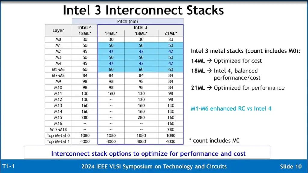
Furthermore, Intel customers can choose from three metal stack configurations: a 14-layer stack focused on cost, an 18-layer stack that balances performance and cost, and a 21-layer stack aimed at high performance.


